
- 澤任訂制
- FST動物實驗器械
- 瑞士ideal-tek鑷子
- 瑞士Dumont鑷子
- Weller
- Techni-Tool
- 瑞士Rubis鑷子
- arosurgica
- Genesee Scientific
- Gilder Grids
-
Entegris
- WEICON
- ACCURIS
- AIMS
- RMC鉆石刀
- Sipel鑷子
- 德國WIHA
-
Si-Mat
- Jokari
- Circuitmedic
-
Glissando病理切片掃描儀
- KNIPEX(凱尼派克)
- Swann-morton
- Cellpoint Scientific
- Swanstrom
- All-spec
-
新華器械
- Excelta
- MENDA
- MEISEI
- Erem
- Regine
-
OPTRASCAN病理掃描儀
- Benchmark
-
IDEAL
- 大龍儀器
- 五洋醫(yī)療
- Hozan(寶山)
- 3M
- Stoelting
- Roboz
-
Diatome鉆石刀
- Fine Science Tools
- PLATO
- NanoSoft
-
Avantama
-
PSI打擊器及配件
- Aptum
- xuron
- SPI
- ASI Instruments
-
上海一恒
-
上海雷磁
- Quantifoil
- 上海方需
- 蘇州六六
-
Hamilton
- ISMART
-
顯微鏡
-
Bonllmann
- AVEN
- 塔望科技
-
瑞典Haglof激光測距儀
- STILLE
-
美國安維迪
- 德國貝朗蛇牌
- Medline
-
蛋白純化系統(tǒng)
-
OHAUS奧豪斯
- 康博特森
- Ossila
-
賽寧(蘇州)生物
- Bernstein
- 潔盟清洗機
-
Ted Pella
-
晶圓切割
-
Omniprobe FIB全鎢取樣針
-
新產(chǎn)品
-
矩陣
-
器械盒
-
切割套裝
-
手套
-
樣品盒
-
吸筆及吸盤
-
晶圓及晶圓盒
-
樹脂及耗材
-
金剛石懸浮液
-
實驗室樣品瓶及杯子
-
實驗室防護
-
石蠟
-
移液器及管
-
離心管及支架
-
計時器
-
玻片儲存盒
-
焊接棒
-
微型小鏟
-
夾持器及微針
-
耳標(biāo)及耗材
-
縫合夾及縫合針
-
放大鏡
-
止血鉗
-
氮化硅膜
-
耗材
-
導(dǎo)電膠及膠帶
-
骨剪及剪刀
-
膠帶及標(biāo)簽
-
顯微載玻片
-
碳粉及碳棒
-
切片機刀片
-
切片模具
-
電鏡載網(wǎng)
-
刀類
-
化學(xué)生物制樣
-
組織標(biāo)記染料
-
鉗子
-
樣品臺
-
拋光布
-
藍(lán)寶石基片
-
吸筆
-
打孔器
-
云母片
-
AFM用品
-
鉆石劃線筆
-
樣品臺盒
-
筆
-
儀器
-
晶圓鉗
-
晶圓切割
- DSI
- Keller
-
Smart Tweezers
- 瑞士PB
-
Microscopes Internat...
- Lattice Gear
-
凱氏定氮儀
- lindstrom
- 美國EMS
-
1-material
-
儀器
- realisticflies
- Boive
- Zivic
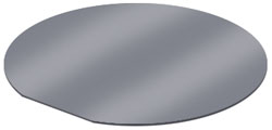 Ultra-Flat Thermal 6" SiO2 Wafer 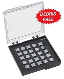 5 x 5mm Diced Ultra-flat Thermal SiO2 Substrates |
Ultra-Flat Thermal SiO2 SubstratesThe Ultra-Flat SiO2 substrates consist of a 200nm thermally grown amorphous SiO2 film on an ultra-flat silicon wafer. SiO2 is one of the most characterized materials and is widely used in semiconductor manufacturing, thin film research and as substrate for growing cells. It can be directly used as substrate for AFM and SEM imaging. The ultra-flat thermal silicon dioxide substrates are available in 6" wafer and conveniently diced 5 x 5mm, 5 x 7mm and 10 x 10mm chips. The 6" wafer is shipped in a 6" wafer carrier, the diced pieces are shipped in a Gel-Pak® box. The special clean dicing process involves coating the wafer with photo resist before dicing and removing it after dicing which produces debris-free SiO2 substrates. All products are packed in class 10 clean room conditions. Properties for thermal SiO2 substrates:
|
|||||||||||||||
|
||||||||||||||||